
Interested in this topic? By joining CR4 you can "subscribe" to
this discussion and receive notification when new comments are added.
 3 3
3
No more Good Answers.
Go to first "Almost" Good Answer
Good Answers:
|


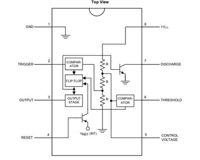
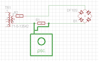
 Re: Charge and discharge time.iming


| Previous in Forum: VSD with Star Delta Starting | Next in Forum: DGTL ISO 2.5KV GATE DRIVER 8SOIC |
Advertisement
Got Something to Say? |
||
Search this Forum |
||
|
Electrical Engineering: |
||
Site Directories |
||
|
Forum Directory Blog Directory User Group Directory RSS Feeds CR4 Rules of Conduct CR4 FAQ Site Glossary Who's Online (52 right now) Show Members |
||
Advertisement
Good Answers:
"Almost" Good Answers: