|
The power-supply industry is currently transitioning from analog to
digital control, especially in high-performance power-supply design. In
fact, digital controllers now control most AC/DC power supplies used in
servers.
Compared to their analog counterparts, digital controllers provide
greater flexibility and performance. But those switching from analog
control to a digital solution face new challenges where continuous
signals are represented by a discrete format: 1 or 0. In this blog
series, I'll provide a practical guide to designing a digital-controlled
power supply.
Digital control fundamentals
As shown in Figure 1, analog control uses discrete
components such as resistors, capacitors and operational amplifiers to
generate a control effort, u(t). This output commands a plant's output,
y(t), to match a reference, r(t), through a sensor, H(s).
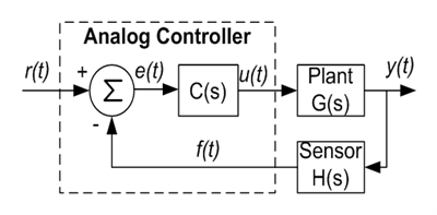
Figure 1: Analog controlled feedback system
Figure 2 illustrates a typical digital-power control
system, with the feedback signal, f(t), sampled and converted to a
digital signal through an analog-to-digital converter (ADC). It is then
compared with a reference to get a digital error signal. A digital
compensator uses this error signal to generate a corresponding
pulse-width modulation (PWM) signal to control the power stage. Compared
to Figure 1, the control principle is the same but the implementation
is different: one is continuous while the other is discrete.
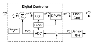
Figure 2: Digital controlled feedback system
A design example
Let's design a simple boost converter using Texas Instruments' UCD3138 controller.
The UCD3138 is
a fully programmable digital power supply controller offering superior
levels of integration and performance in a single chip solution. The
flexible nature makes it suitable for a wide variety of power conversion
applications, include power factor correction (PFC), LLC resonant
converter, phase shifted full bridge, etc. In addition, multiple
peripherals inside the device are specifically optimized to enhance the
performance of AC/DC and isolated DC/DC applications and reduce
component count.
Figure 3 is a block diagram of a UCD3138-controlled
boost converter. The signal interface is straightforward: the converter
output voltage is attenuated and connected to the control loop feedback
input pin. It is then compared with an internal programmable reference
to get an error. The error is then sent to an error ADC (EADC) and
digitized. This digital error signal then goes through a
proportional-integral-derivative (PID) digital compensator, and the
output of the PID generates the corresponding PWM duty cycle. All the
compensations are internal, no any external compensation circuit needed.
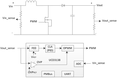
Figure 3: A UCD3138-controlled boost converter block diagram
In addition, UCD3138 has
built in analog comparators with programmable reference, it can be used
to implement fast overvoltage protection (OVP). The analog comparator
will be trigged if the sensed Vout signal is higher than a pre-defined
threshold, all the PWM signals will shut down to protect the power
supply. The input voltage can also be measured by ADC for input brownout
protection.
Close the loop
When talking about loop control, pole/zero are common terms for
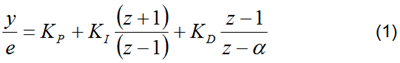
analog power engineers, but the digital control world usually uses PID. A
traditional PID is combined with an extra ɑ in the UCD3138 to provide a two-pole two-zero digital compensator, as shown in Figure 4.

Figure 4: UCD3138 PID structure
Equation 1 calculates the transfer function for this PID in the z domain:
Both KP, KI, KD and ɑ are
programmable and can be adjusted on the fly; this means that the control
loop can be dynamically changed based on the operational condition to
achieve best performance. Nonlinear PID control is also supported for
fast transient response.
Just as in analog power-supply designs, the goal for control-loop
designs is to find the right pole/zero such that the system has a
desired loop bandwidth and enough stability margins. Here's a typical
sequence to design a UCD3138 control loop:
- Derive the small-signal model of the power stage.
- Choose the appropriate KP, KI, KD and ɑ such that the loop has the desired bandwidth and enough stability margins.
- Load KP, KI, KD and ɑ into the UCD3138 and turn on the power converter.
- Fine-tune KP, KI, KD and ɑ until
the converter performance meets your desired specifications. For
example, the Vout deviation during load transient should within a
specific range.
- Use a frequency analyzer to measure the actual loop bandwidth and
stability margins. If they do not meet your desired specifications,
repeat step 4.
See the additional resources section for more information about how the UCD3138 PID controller works, and the design examples of how to tune the control loop with the help of a frequency analyzer.
In the case that you are familiar with the traditional analog
compensator, as shown in Figure 5, and you want to keep the same
compensation in your digital design, you can use Equations 2, 3, 4 and 5
to translate the poles/zeros in the time domain into KP, KI, KD and ɑ in the z domain.
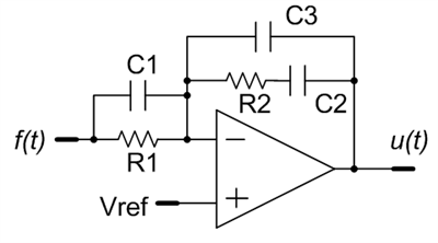
Figure 5: Traditional analog compensator
Now you have a UCD3138-controlled power converter ready to be tested. In part 2, I'll talk about how to write firmware to make it work.
Additional Resources
Editor's note: This is a sponsored blog post by Texas Instruments PWR.
| 


 Re: Designing A Digital-controlled Power Supply
"Almost" Good Answers: